Chemical Analysis & Analytical Instruments


Precision systems, including closed loop systems, with high resolution time domain analysis or frequency domain analysis all require precision and wide bandwidth. Our precision signal chains expedite component selection and reduce design time.

- Instrumentation & Measurement
- Automated Test Equipment
- Battery Formation & Test
- Chemical Analysis & Analytical Instruments
-
- Instrumenting 5G
- Data Acquisition
- Precision Measurement
- DC Sources & Power Supplies
- Parametric Measurement
- Impedance Measurement & Analysis
- Oscilloscopes & Digitizers
- Precision Signal Analyzers
- RF Signal Analyzers & Vector Network Analyzers
- Signal Generators (Audio through RF)
- RF Frequency & Power Measurement
- Communications Test Equipment
- Switching Matrices
- Power Circuits for Instrumentation
- Weigh Scales
- High Temperature
Chemical and analytical instruments are used to test and measure the real world for human benefit. For example, this includes applications such as environmental air and water quality, material and product analysis for higher quality goods, oil and geophysical exploration, and deepening scientific discovery. Chemical analysis involves detection of light and the use of charged ion beams, redox reactions, and other technologies. Analysis methods including spectroscopy, spectrometry, and electrochemistry which implement these technologies are selected based on sample type and measurement characteristics. Accurate, high-confidence detection, identification, and characterization depends on precise sensing capability and electronics. ADI’s best-in-class signal chain, sensor, power, and processor solutions ensure that your limit of detect (LOD) and accuracy are not restricted by your electronics design.

Featured Products (11)
ADUCM355

The ADuCM355 is an on-chip system that controls and measures electrochemical sensors and biosensors. The ADuCM355 is an ultralow power, mixed-signal microcontroller based on the Arm® Cortex™-M3 processor. The device features current, voltage, and impedance measurement capability.
The ADuCM355 features a 16-bit, 400 kSPS, multichannel successive approximation register (SAR) analog-to-digital converter (ADC) with input buffers, built-in antialias filter (AAF), and programmable gain amplifier (PGA). The current inputs include three transimpedance amplifiers (TIA) with programmable gain and load resistors for measuring different sensor types. The analog front end (AFE) also contains two low power amplifiers designed specifically for potentiostat capability to maintain a constant bias voltage to an external electrochemical sensor. The noninverting inputs of these two amplifiers are controlled by on-chip, dual output digital-to-analog converters (DACs). The analog outputs include a high speed DAC and output amplifier designed to generate an ac signal.
The ADC operates at conversion rates up to 400 kSPS with an input range of −0.9 V to +0.9 V. An input mux before the ADC allows the user to select an input channel for measurement. These input channels include three external current inputs, multiple external voltage inputs, and internal channels. The internal channels allow diagnostic measurements of the internal supply voltages, die temperature, and reference voltages.
Two of the three voltage DACs are dual output, 12-bit string DACs. One output per DAC controls the noninverting input of a potentiostat amplifier, and the other controls the noninverting input of the TIA.
The third DAC (sometimes referred to as the high speed DAC) is designed for the high power TIA for impedance measurements. The output frequency range of this DAC is up to 200 kHz.
A precision 1.82 V and 2.5 V on-chip reference source is available. The internal ADC and voltage DAC circuits use this on-chip reference source to ensure low drift performance for all peripherals.
The ADuCM355 integrates a 26 MHz Arm Cortex-M3 processor, which is a 32-bit reduced instruction set computer (RISC) machine. The Arm Cortex-M3 processor also has a flexible multichannel direct memory access controller (DMA) supporting two independent serial peripheral interface (SPI) ports, universal asynchronous receiver/transmitter (UART), and I2C communication peripherals. The ADuCM355 has 128 kB of nonvolatile flash/EE memory and 64 kB of single random access memory (SRAM) integrated on-chip.
The digital processor subsystem is clocked from a 26 MHz on-chip oscillator. The oscillator is the source of the main digital die system clock. Optionally, a 26 MHz phase-locked loop (PLL) can be used as the digital system clock. This clock can be internally subdivided so that the processor operates at a lower frequency and saves power. A low power, internal 32 kHz oscillator is available and can clock the timers. The ADuCM355 includes three general-purpose timers, a wake-up timer (which can be used as a general-purpose timer), and a system watchdog timer.
The analog subsystem has a separate 16 MHz oscillator used to clock the ADC, DACs, and other digital logic on the analog die. The analog die also contains a separate 32 kHz, low power oscillator to clock a watchdog timer on the analog die. Both the 32 kHz oscillator and this watchdog are independent from the digital die oscillators and system watchdog timer.
A range of communication peripherals can be configured as required in a specific application. These peripherals include UART, I2C, two SPI ports, and general-purpose input/output (GPIO) ports. The GPIOs, combined with the general-purpose timers, can be combined to generate a pulse-width modulation (PWM) type output.
Nonintrusive emulation and program download are supported via the serial wire debug port (SW-DP) interface.
The ADuCM355 operates from a 2.8 V to 3.6 V supply and is specified over a temperature range of −40°C to +85°C. The chip is packaged in a 72-lead, 6 mm × 5 mm land grid array (LGA) package.
Note that, throughout this data sheet, multifunction pins, such as P0.0/SPI0_CLK, are referred to either by the entire pin name or by a single function of the pin, for example, P0.0, when only that function is relevant.
Applications
- Gas detection
- Food quality
- Environmental sensing (air, water, and soil)
- Blood glucose meters
- Life sciences and biosensing analysis
- Bioimpedance measurements
- General Amperometry, voltammetry, and impedance spectroscopy functions
Applications
Intelligent Buildings
- Environmental Monitoring Solutions
ADA4530-1

The ADA4530-1 is a femtoampere (10−15 A) level input bias current operational amplifier suitable for use as an electrometer that also includes an integrated guard buffer. It has an operating voltage range of 4.5 V to 16 V, enabling it to operate in conventional 5 V and 10 V single supply systems as well as ±2.5 V and ±5 V dual supply systems.
It provides ultralow input bias currents that are production tested at 25°C and at 125°C to ensure the device meets its performance goals in user systems. The integrated guard buffer isolates the input pins from leakage in the printed circuit board (PCB), minimizes board component count, and enables easy system design. The ADA4530-1 is available in an industry-standard surface-mount 8-lead SOIC package with a unique pinout optimized to prevent signals from coupling between the sensitive input pins, the power supplies, and the output pin while enabling easy routing of the guard ring traces.
The ADA4530-1 also offers low offset voltage, low offset drift, and low voltage and current noise needed for the types of applications that require such low leakages.
To maximize the dynamic range of the system, the ADA4530-1 has a rail-to-rail output stage that can typically drive to within 30 mV of the supply rails under a 10 kΩ load.
The ADA4530-1 operates over the −40°C to +125°C industrial temperature range and is available in an 8-lead SOIC package.
Applications
- Laboratory and analytical instrumentation: spectrophotometers, chromatographs, mass spectrometers, and potentiostatic and amperostatic coulometry
- Instrumentation: picoammeters and coulombmeters
- Transimpedance amplifier (TIA) for photodiodes, ion chambers, and working electrode measurements
- High impedance buffering for chemical sensors and capacitive sensors
Applications
ADA4350

The ADA4350 is an analog front end for photodetectors or other sensors whose output produces a current proportional to the sensed parameter or voltage input applications where the system requires the user to select between very precise gain levels to maximize the dynamic range.
The ADA4350 integrates a FET input amplifier, a switching network, and an ADC driver with all functions controllable via a serial peripheral interface (SPI) or parallel control logic into a single IC. The FET input amplifier has very low voltage noise and current noise making it an excellent choice to work with a wide range of photodetectors, sensors, or precision data acquisition systems.
Its switching network allows the user individual selection of up to six different, externally configurable feedback networks; by using external components for the feedback network, the user can more easily match the system to their desired photodetector or sensor capacitance. This feature also allows the use of low thermal drift resistors, if required.
The design of the switches minimizes error sources so that they add virtually no error in the signal path. The output driver can be used in either single-ended or a differential mode and is ideal for driving the input of an ADC.
The ADA4350 can operate from a single +3.3 V supply or a dual ±5 V supply, offering user flexibility when choosing the polarity of the detector. It is available in a Pb-free, 28-lead TSSOP package and is specified to operate over the −40°C to +85°C temperature range. Multifunction pin names may be referenced by their relevant function only.
Applications
- Current to voltage (I to V) conversions
- Photodiode preamplifiers
- Chemical analyzers
- Mass spectrometry
- Molecular spectroscopy
- Laser/LED receivers
- Data acquisition systems
Applications
Markets
AD7175-2

The AD7175-2 is a low noise, fast settling, multiplexed, 2-/4- channel (fully/pseudo differential) Σ-Δ analog-to-digital converter (ADC) for low bandwidth inputs. It has a maximum channel scan rate of 50 kSPS (20 µs) for fully settled data. The output data rates range from 5 SPS to 250 kSPS.
The AD7175-2 integrates key analog and digital signal conditioning blocks to allow users to configure an individual setup for each analog input channel in use. Each feature can be user selected on a per channel basis. Integrated true rail-to-rail buffers on the analog inputs and external reference inputs provide easy to drive high impedance inputs. The precision 2.5 V low drift (2 ppm/°C) band gap internal reference (with output reference buffer) adds embedded functionality to reduce external component count.
The digital filter allows simultaneous 50 Hz/60 Hz rejection at 27.27 SPS output data rate. The user can switch between different filter options according to the demands of each channel in the application. The ADC automatically switches through each selected channel. Further digital processing functions include offset and gain calibration registers, configurable on a per channel basis.
The device operates with a 5 V AVDD1, or ±2.5 V AVDD1/AVSS, and 2 V to 5 V AVDD2 and IOVDD supplies. The specified operating temperature range is −40°C to +105°C. The AD7175-2 is in a 24-lead TSSOP package.
Applications
- Process control: PLC/DCS modules
- Temperature and pressure measurement
- Medical and scientific multichannel instrumentation
- Chromatography
Applications
Intelligent Buildings
- Building Utilities
AD7124-4

The AD7124-4 is a low power, low noise, completely integrated analog front end for high precision measurement applications. The device contains a low noise, 24-bit Σ-Δ analog-to-digital converter (ADC), and can be configured to have 4 differential inputs or 7 single-ended or pseudo differential inputs. The onchip low gain stage ensures that signals of small amplitude can be interfaced directly to the ADC.
One of the major advantages of the AD7124-4 is that it gives the user the flexibility to employ one of three integrated power modes. The current consumption, range of output data rates, and rms noise can be tailored with the power mode selected. The device also offers a multitude of filter options, ensuring that the user has the highest degree of flexibility.
The AD7124-4 can achieve simultaneous 50 Hz and 60 Hz rejection when operating at an output data rate of 25 SPS (single cycle settling), with rejection in excess of 80 dB achieved at lower output data rates.
The AD7124-4 establishes the highest degree of signal chain integration. The device contains a precision, low noise, low drift internal band gap reference, and also accepts an external differential reference, which can be internally buffered. Other key integrated features include programmable low drift excitation current sources, burnout currents, and a bias voltage generator, which sets the common-mode voltage of a channel to AVDD/2. The low-side power switch enables the user to power down bridge sensors between conversions, ensuring the absolute minimal power consumption of the system. The device also allows the user the option of operating with either an internal clock or an external clock.
The integrated channel sequencer allows several channels to be enabled simultaneously, and the AD7124-4 sequentially converts on each enabled channel, simplifying communication with the device. As many as 16 channels can be enabled at any time; a channel being defined as an analog input or a diagnostic such as a power supply check or a reference check. This unique feature allows diagnostics to be interleaved with conversions.
The AD7124-4 also supports per channel configuration. The device allows eight configurations or setups. Each configuration consists of gain, filter type, output data rate, buffering, and reference source. The user can assign any of these setups on a channel by channel basis.
The AD7124-4 also has extensive diagnostic functionality integrated as part of its comprehensive feature set. These diagnostics include a cyclic redundancy check (CRC), signal chain checks, and serial interface checks, which lead to a more robust solution. These diagnostics reduce the need for external components to implement diagnostics, resulting in reduced board space needs, reduced design cycle times, and cost savings. The failure modes effects and diagnostic analysis (FMEDA) of a typical application has shown a safe failure fraction (SFF) greater than 90% according to IEC 61508.
The device operates with a single analog power supply from 2.7 V to 3.6 V or a dual 1.8 V power supply. The digital supply has a range of 1.65 V to 3.6 V. It is specified for a temperature range of −40°C to +105°C. The AD7124-4 is housed in a 32-lead LFCSP package or a 24-lead TSSOP package.
Applications
- Temperature measurement
- Pressure measurement
- Industrial process control
- Instrumentation Smart transmitters
- Smart transmitters
Applications
Intelligent Buildings
- Building Automation Systems
- Building Controllers and Networks
- Building Utilities
- Building Safety and Security Solutions
AD7798

The AD7798/AD7799 are low power, low noise, complete analog front ends for high precision measurement applications. The AD7798/AD7799 contains a low noise, 16-/24-bit Σ-Δ ADC with three differential analog inputs. The on-chip, low noise instrumentation amplifier means that signals of small amplitude can be interfaced directly to the ADC. With a gain setting of 64, the rms noise is 27 nV for the AD7799 and 40 nV for the AD7798 when the update rate equals 4.17 Hz.
On-chip features include a low-side power switch, reference detect, programmable digital output pins, burnout currents, and an internal clock oscillator. The output data rate from the part is software-programmable and can be varied from 4.17 Hz to 470 Hz.
The part operates with a power supply from 2.7 V to 5.25 V. The AD7798 consumes a current of 300 μA typical, whereas the AD7799 consumes 380 μA typical. Both devices are housed in a 16-lead TSSOP package.
APPLICATIONS
- Weigh scales
- Pressure measurement
- Strain gauge transducers
- Gas analysis
- Industrial process control
- Instrumentation
- Portable instrumentation
- Blood analysis
- Smart transmitters
- Liquid/gas chromotography 6-digit DVM
Applications
AD7980

The SPI-compatible serial interface also features the ability, using the SDI input, to daisy-chain several ADCs on a single, 3-wire bus and provides an optional busy indicator. It is compatible with 1.8 V, 2.5 V, 3 V, or 5 V logic, using the separate supply VIO.
The AD7980 is housed in a 10-lead MSOP or a 10-lead QFN (LFCSP) with operation specified from −40°C to +125°C.
APPLICATIONS- Automated test equipment
- Data acquisition systems
- Medical instruments
- Machine automation
Applications
AD5791

The AD57911 is a single 20-bit, unbuffered voltage-output DAC that operates from a bipolar supply of up to 33 V. The AD5791 accepts a positive reference input in the range 5 V to VDD – 2.5 V and a negative reference input in the range VSS + 2.5 V to 0 V. The AD5791 offers a relative accuracy specification of ±1 LSB max, and operation is guaranteed monotonic with a ±1 LSB differential nonlinearity (DNL) maximum specification.
The device uses a versatile 3-wire serial interface that operates at clock rates up to 35 MHz and that is compatible with standard serial peripheral interface (SPI), QSPI™, MICROWIRE™, and DSP interface standards. The device incorporates a power-on reset circuit that ensures the DAC output powers up to 0 V and in a known output impedance state and remains in this state until a valid write to the device takes place. The device provides an output clamp feature that places the output in a defined load state.
Product Highlights
- 1 ppm Accuracy.
- Wide Power Supply Range up to ±16.5 V.
- Operating Temperature Range: −40°C to +125°C.
- Low 7.5 nV/√Hz Noise Spectral Density.
- Low 0.05 ppm/°C Temperature Drift.
- Medical instrumentation
- Test and measurement
- Industrial control
- High end scientific and aerospace instrumentation
1 Protected by U.S. Patent No. 7,884,747. Other patents pending.
Applications
ADAQ7980

The ADAQ7980/ADAQ7988 are 16-bit analog-to-digital converter (ADC) μModule® data acquisition systems that integrate four common signal processing and conditioning blocks into a system in package (SiP) design that supports a variety of applications. These devices contain the most critical passive components, eliminating many of the design challenges associated with traditional signal chains that use successive approximation register (SAR) ADCs. These passive components are crucial to achieving the specified device performance.
The ADAQ7980/ADAQ7988 contain a high accuracy, low power, 16-bit SAR ADC, a low power, high bandwidth, high input impedance ADC driver, a low power, stable reference buffer, and an efficient power management block. Housed within a tiny, 5 mm × 4 mm LGA package, these products simplify the design process for data acquisition systems. The level of system integration of the ADAQ7980/ADAQ7988 solves many design challenges, while the devices still provide the flexibility of a configurable ADC driver feedback loop to allow gain and/or common-mode adjustments. A set of four device supplies provides optimal system performance; however, single-supply operation is possible with minimal impact on device operating specifications.
The ADAQ7980/ADAQ7988 integrate within a compact, integrated circuit (IC)-like form factor key components commonly used in data acquisition signal chain designs. The μModule family transfers the design burden of component selection, optimization, and layout from designer to device, shortening overall design time, system troubleshooting, and ultimately improving time to market.
The serial peripheral interface (SPI)-compatible serial interface features the ability to daisy-chain multiple devices on a single, 3-wire bus and provides an optional busy indicator. The user interface is compatible with 1.8 V, 2.5 V, 3 V, or 5 V logic.
Specified operation of these devices is from −55°C to +125°C.
Applications
- Automated test equipment (ATE)
- Battery powered instrumentation
- Communications
- Data acquisition
- Process control
- Medical instruments
Applications
ADUCM350

The ADuCM350 is a configurable Impedance Converter and Potentiostat with current and voltage measurement capability for both Electrochemical sensors and Biosensors. It is a complete, coin cell powered, high precision, MCU integrated solution for portable device applications such as point-of-care diagnostics and body-worn devices for monitoring vital signs.
The ADuCM350 analog front end (AFE) features a 16-bit, precision, 160 kSPS analog-to-digital converter (ADC); 0.17% precision voltage reference; 12-bit, no missing codes digital-to-analog converter (DAC); and a reconfigurable ultralow leakage switch matrix. It has 4 voltage measurement channels, up to 8 current measurement channels and an impedance measurement DFT engine. The ADuCM350 also includes an ARM Cortex-M3-based processor, memory, and all I/O connectivity to support portable meters with display, USB communication, and active sensors. The ADuCM350 is available in a 120-lead, 8 mm × 8 mm CSP_BGA and operates from −40°C to +85°C.
To support extremely low dynamic and hibernate power management, the ADuCM350 provides a collection of power modes and features, such as dynamic and software controlled clock gating and power gating. The AFE is connected to the ARM Cortex-M3 via an advanced high performance bus (AHPB) slave interface on the advanced microcontroller bus architecture (AMBA) matrix, as well as direct memory access (DMA) and interrupt connections.
APPLICATIONS
- Point-of-care diagnostics
- Body-worn devices for monitoring vital signs
- Amperometric, voltametric, and impedometric measurements
Applications
ADUCM360

The ADuCM360/ADuCM361 contain an on-chip 32 kHz oscillator and an internal 16 MHz high frequency oscillator. The high frequency oscillator is routed through a programmable clock divider from which the operating frequency of the processor core clock is generated. The maximum core clock speed is 16 MHz; this speed is not limited by operating voltage or temperature.
The microcontroller core is a low power ARM Cortex-M3 processor, a 32-bit RISC machine that offers up to 20 MIPS peak performance. The Cortex-M3 processor incorporates a flexible, 11-channel DMA controller that supports all wired communica-tion peripherals (SPI, UART, and I2C). Also integrated on chip are 128 kB of nonvolatile Flash/EE memory and 8 kB of SRAM.
The analog subsystem consists of dual ADCs, each connected to a flexible input mux. Both ADCs can operate in fully differential and single-ended modes. Other on-chip ADC features include dual programmable excitation current sources, diagnostic current sources, and a bias voltage generator of AVDD_REG/2 (900 mV) to set the common-mode voltage of an input channel. A low-side internal ground switch is provided to allow power-down of an external circuit (for example, a bridge circuit) between conversions.
The ADCs contain two parallel filters: a sinc3 or sinc4 filter in parallel with a sinc2 filter. The sinc3 or sinc4 filter is used for precision measurements. The sinc2 filter is used for fast measure-ments and for the detection of step changes in the input signal.
The devices contain a low noise, low drift internal band gap ref-erence, but they can be configured to accept one or two external reference sources in ratiometric measurement configurations. An option to buffer the external reference inputs is provided on chip. A single-channel buffered voltage output DAC is also provided on chip.
The ADuCM360/ADuCM361 integrate a range of on-chip peripherals, which can be configured under microcontroller software control as required in the application. The peripherals include UART, I2C, and dual SPI serial I/O communication controllers; a 19-pin GPIO port; two general-purpose timers; a wake-up timer; and a system watchdog timer. A 16-bit PWM controller with six output channels is also provided.
The ADuCM360/ADuCM361 are specifically designed to operate in battery-powered applications where low power operation is critical. The microcontroller core can be configured in a normal operating mode that consumes 290 μA/MHz (including flash/ SRAM IDD). An overall system current consumption of 1 mA can be achieved with both ADCs on (input buffers off), PGA gain of 4, one SPI port on, and all timers on.
The ADuCM360/ADuCM361 can be configured in a number of low power operating modes under direct program control, including a hibernate mode (internal wake-up timer active) that consumes only 4 μA. In hibernate mode, peripherals such as external interrupts or the internal wake-up timer can wake up the device. This mode allows the part to operate with ultralow power and still respond to asynchronous external or periodic events.
APPLICATIONS
- Industrial automation and process control
- Intelligent precision sensing systems
- 4 mA to 20 mA loop-powered smart sensor systems
- Medical devices, patient monitoring
Applications
Signal Chains
(9)
Interactive Signal Chains


Reference Designs
CN0429

Gas detection instruments are used in a wide range of applications ranging from home air quality measurement devices to industrial solutions for detecting toxic gases. Many of these instruments use electrochemical gas sensors. This sensor technology requires specialized front-end circuitry for biasing and measurement.
By utilizing built-in diagnostics features (such as impedance spectroscopy or bias voltage pulsing and ramping) it is possible to inspect sensor health, compensate for accuracy drift due to aging or temperature, and estimate the remaining lifetime of the sensor right at the edge of the sensor network without user intervention. This functionality allows smart, accurate sensor replacement at the individual edge nodes. An integrated, ultra low power microcontroller directly biases the electrochemical gas sensor and runs onboard diagnostic algorithms.
The circuit shown in Figure 1 shows how an electrochemical gas sensor is connected to the potentiostat circuit and how it is biased and measured. Common 2-lead, 3-lead, and 4-lead electrochemical gas sensors can be used interchangeably. The integration of this signal chain dramatically reduces cost, size, complexity, and power consumption at the sensor node.

Applicable Parts
ADUCM355
Precision Analog Microcontroller with Chemical Sensor Interface
Applications
Instrumentation & Measurement
- Chemical Analysis & Analytical Instruments
CN0428
Many important liquid analyses like pH rely on electrochemistry, a branch of chemistry that characterizes the behavior of reduction-oxidation (redox) reactions by measuring the transfer of electrons from one reactant to another. Electrochemical techniques can be used directly or indirectly to detect several important parameters that affect water quality, including chemical indicators, biological and bacteriological indicators and even some low level contaminants like heavy metals. Many of these indicative measurements are pertinent to determining important quality parameters of the tested analyte.
The circuit shown in Figure 1 is a modular sensing platform that allows the user to design a flexible electrochemical water quality measurement solution. Its high level of integration enables an electrochemical measurement platform applicable to a variety of water quality probes including pH, oxidation reduction potential (ORP), and conductivity cells.
The system allows up to four probes to be connected at one time for different water quality measurements.


Applicable Parts
Applications
CN0409

The circuit shown in Figure 1 uses a photometric front end and a network of 860 nm infrared (IR) emitters and silicon PIN photodiodes to achieve a water turbidity measurement system. Turbidity is an important water quality indicator for the presence of dispersed or suspended solids, which affects potable water and environmental conditions. Turbidity is a qualitative characteristic imparted by how these suspended solids obstruct the transmittance of light. Turbidity is not a direct measure of suspended particles in water but rather a measure of the scattering effect that such particles have on light.

The system can measure low to high water turbidity levels ranging from 0 FTU to 1000 FTU. The IR LED and photodiode network is arranged in such a way that it can support two of the most recognized turbidity measurement standards: ISO7027 (both ratio and nonratio) and the GLI method. With three-point calibration, the typical accuracy that the system can achieve is ±0.50 FTU or ±5% of the reading, whichever is greater. This accuracy combined with the 0.05 FTU noise level makes the measurements obtained using this system very reliable.
The ADPD105 ambient light rejection feature makes this circuit ideal for applications where accurate, robust, and noncontact turbidity measurements are critical. Applications include chemical analysis and environmental monitoring of natural bodies of water (such as wastewater and drinking water).
The printed circuit board (PCB) is designed in an Arduino shield-compatible form factor and directly interfaces to the EVAL-ADICUP360 Arduino form factor-compatible platform board for rapid prototyping.
Applicable Parts
Applications
Instrumentation & Measurement
- Chemical Analysis & Analytical Instruments
CN0338

The circuit shown in Figure 1 is a complete thermopile-based gas sensor using the nondispersive infrared (NDIR) principle. This circuit is optimized for CO2 sensing, but can also accurately measure the concentration of a large number of gases by using thermopiles with different optical filters.

The printed circuit board (PCB) is designed in an Arduino shield form factor and interfaces to the EVAL-ADICUP360 Arduino-compatible platform board. The signal conditioning is implemented with the AD8629 and the ADA4528-1 low noise amplifiers and the ADuCM360 precision analog microcontroller, which contains programmable gain amplifiers, dual 24-bit Σ-Δ analog-to-digital converters (ADCs), and an ARM Cortex-M3 processor.
Applicable Parts
AD8629
Zero Drift, Single-Supply, R/R, Input/Output Operational Amplifier
ADA4528-1
Precision, Ultralow Noise, RRIO, Zero-Drift Single Op Amp
ADP7105
20 V, 500 mA, Low Noise LDO Regulator with Soft Start
ADuCM362
Low Power, Precision Analog Microcontroller with Dual Sigma-Delta ADCs, ARM Cortex-M3
ADuCM363
Low Power, Precision Analog Microcontroller with Single Sigma-Delta ADC, ARM Cortex-M3
Applications
Intelligent Buildings
- HVAC Systems Technologies
- Environmental Monitoring Solutions
CN0383

The circuit shown in Figure 1 is an integrated 2-wire, 3-wire, or 4-wire resistance temperature detector (RTD) system based on the AD7124-4/AD7124-8 low power, low noise, 24-bit Σ-Δ analog-to-digital converter (ADC) optimized for high precision measurement applications.

This circuit note uses a Class B Pt100 RTD sensor with an accuracy of ±0.3°C at 0°C but it can support other classes such as Class A, Class AA, 1/3 DIN, or 1/10 DIN that are higher accuracy RTDs. This circuit also has provision for Pt1000 RTDs that are useful in low power applications.
The AD7124-4/AD7124-8 can achieve high resolution, low nonlinearity, and low noise performance as well as high 50 Hz and 60 Hz rejection, suitable for industrial RTD systems. The typical peak to peak resolution of the system is 0.0043°C (17.9 bits) for full power mode, sinc4 filter selected, at an output data rate of 50 SPS, and 0.0092°C (16.8 bits) for low power mode, post filter selected, at an output data rate of 25 SPS. These settings show that the system accuracy is significantly better than the sensor accuracy.
The AD7124-4/AD7124-8 integrate several important system building blocks required to support RTD measurements. Functions, including programmable excitation current sources and a programmable gain amplifier (PGA), excite and gain the RTD, respectively, which allows direct interfacing with the sensor and simplifies the design while reducing cost and power consumption.
Several options of the on-chip digital filtering and three integrated power modes, where the current consumption, range of output data rates, settling time, and rms noise are optimized, provide application flexibility. The current consumed in low power mode is only 255 μA and in full power mode is 930 μA. In power-down mode, the complete ADC along with its auxiliary functions are powered down so that the AD7124-4/AD7124-8 consume 1 μA typical. The power options make the AD7124-4/AD7124-8 suitable for nonpower critical applications, such as input modules, and also for low power applications, such as loop-powered smart transmitters where the complete transmitter must consume less than 4 mA.
The AD7124-4/AD7124-8 also have extensive diagnostic functionality integrated as part of its comprehensive feature set. This functionality can be used to check that the voltage level on the analog pins are within the specified operating range. These devices also include a cyclic redundancy check (CRC) on the serial peripheral interface (SPI) bus and signal chain checks, which leads to a more robust solution. These diagnostics reduce the need for external components to implement diagnostics, resulting in a smaller solution size, reduced design cycle times, and cost savings.
Applicable Parts
Applications
CN0384

The circuit shown in Figure 1 is an integrated thermocouple measurement system based on the AD7124-4/AD7124-8 low power, low noise, 24-bit, Σ-Δ analog-to-digital converter (ADC), optimized for high precision measurement applications. Thermocouple measurements using this system show an overall system accuracy of ±1°C over a measurement temperature range of −50°C to +200°C . Typical noise free code resolution of the system is approximately 15 bits.

The AD7124-4 can be configured for 4 differential or 7 pseudo differential input channels, while the AD7124-8 can be configured for 8 differential or 15 pseudo differential channels. The on-chip low noise programmable gain array (PGA) ensures that signals of small amplitude can be interfaced directly to the ADC.
The AD7124-4/AD7124-8 establishes the highest degree of signal chain integration, which includes programmable low drift excitation current sources, bias voltage generator, and internal reference. Therefore, the design of a thermocouple system is simplified when the AD7124-4/AD7124-8 is used because most of the required system building blocks are included on-chip.
The AD7124-4/AD7124-8 gives the user the flexibility to employ one of three integrated power modes, where the current consumption, range of output data rates, and rms noise are tailored with the power mode selected. The current consumed by the AD7124-4/AD7124-8 is only 255 μA in low power mode and 930 μA in full power mode. The power options make the device suitable for non-power critical applications, such as input/output modules, and also for low power applications, such as loop-powered smart transmitters where the complete transmitter must consume less than 4 mA.
The device also has a power-down option. In power-down mode, the complete ADC along with its auxiliary functions are powered down so that the device consumes 1 μA typical. The AD7124-4/AD7124-8 also has extensive diagnostic functionality integrated as part of its comprehensive feature set.
Applicable Parts
Applications
CN0407

The system functional diagram in Figure 1 is a precision analog front end for measurement of current down to the femtoampere range. This industry-leading solution is ideal for chemical analyzers and laboratory grade instrument where an ultrahigh sensitivity analog front end is required for signal conditioning current output sensors such as photodiodes, photomultiplier tubes, and Faraday cups. Applications that can use this solution include mass spectrometry, chromatography, and coulometry.
The EVAL-CN0407-SDPZ provides a reference design for real-world application by partitioning the system into a low-leakage mezzanine board and a data acquisition board. The input signal conditioning is implemented with the ADA4530-1 on the mezzanine board. The ADA4530-1 is an electrometer-grade amplifier with ultralow input bias current of 20 fA maximum at 85°C. A guard buffer is integrated on the chip to isolate the input pins from leakage to the printed circuit board (PCB). The default amplifier configuration is in the transimpedance mode with a 10 GΩ glass resistor and a metal shield that prevents leakage current from entering any of the high impedance paths on the board. In addition, the mezzanine board includes unpopulated resistor and capacitor pads to allow prototyping with surface-mount feedback resistors as well as other input configurations.
The data acquisition board uses an AD7172-2 24-bit Σ-Δ analog-to-digital-converter (ADC) and is powered from a single 9 V dc supply. The on-board supply generates all necessary voltages required to power both boards. The board connects to a PC via the SDP-S board (EVAL-SDP-CS1Z) and uses digital isolation to prevent noise from the USB bus or ground loops from degrading low current measurements.

Applicable Parts
ADUM3151
3.75 kV, 7-Channel, SPIsolator Digital Isolators for SPI (with 2/1 Aux channel directionality)
ADP7182
–28 V, −200 mA, Low Noise, Linear Regulator
ADR4525
Ultra-Low-Noise, High-Accuracy 2.5V Voltage Reference
AD7172-2
Low Power, 24-Bit, 31.25 kSPS, Sigma-Delta ADC with True Rail-to-Rail Buffers
ADA4530-1
Femtoampere Input Bias Current Electrometer Amplifier
Applications
CN0363

The circuit shown in Figure 1 is a dual-channel colorimeter featuring a modulated light source transmitter, programmable gain transimpedance amplifiers on each channel, and a very low noise, 24-bit Σ-Δ analog-to-digital converter (ADC). The output of the ADC connects to a standard FPGA mezzanine card. The FPGA takes the sampled data from the ADC and implements a synchronous detection algorithm.

By using modulated light and digital synchronous detection rather than a constant (dc) source, the system strongly rejects any noise sources at frequencies other than the modulation frequency, providing excellent accuracy.
The dual-channel circuit measures the ratio of light absorbed by the liquids in the sample and reference containers at three different wavelengths. This measurement forms the basis of many chemical analysis and environmental monitoring instruments used to measure concentrations and characterize materials through absorption spectroscopy.
Applicable Parts
AD7175-2
24-Bit, 250 kSPS, Sigma-Delta ADC with 20 µs Settling and True Rail-to-Rail Buffers
ADA4528-1
Precision, Ultralow Noise, RRIO, Zero-Drift Single Op Amp
AD8615
Precision 20 MHz CMOS Single RRIO Operational Amplifier
AD5201
33-Position Digital Potentiometer
ADA4805-1
0.2 µV/°C Offset Drift, 105 MHz Low Power, Low Noise, Rail-to-Rail Amplifier
ADG633
CMOS, ±5 V/+5 V/+3 V, Triple SPDT Switch
ADG733
CMOS, 2.5 Ω Low Voltage, Triple SPDT Switch
ADG704
CMOS, Low Voltage 2.5 Ω 4-Channel Multiplexer
ADG819
0.5 Ω CMOS 1.8 V to 5.5 V 2:1 Mux/SPDT Switch with BBM Switching Action
Applications
CN0359

The circuit shown in Figure 1 is a completely self-contained, microprocessor controlled, highly accurate conductivity measurement system ideal for measuring the ionic content of liquids, water quality analysis, industrial quality control, and chemical analysis.
A carefully selected combination of precision signal conditioning components yields an accuracy of better than 0.3% over a conductivity range of 0.1 μS to 10 S (10 MΩ to 0.1 Ω) with no calibration requirements.
Automatic detection is provided for either 100 Ω or 1000 Ω platinum (Pt) resistance temperature devices (RTDs), allowing the conductivity measurement to be referenced to room temperature.
The system accommodates 2- or 4-wire conductivity cells, and 2-, 3-, or 4-wire RTDs for added accuracy and flexibility.
The circuit generates a precise ac excitation voltage with minimum dc offset to avoid a damaging polarization voltage on the conductivity electrodes. The amplitude and frequency of the ac excitation is user-programmable.
An innovative synchronous sampling technique converts the peak-to-peak amplitude of the excitation voltage and current to a dc value for accuracy and ease in processing using the dual, 24-bit Σ-Δ ADC contained within the precision analog microcontroller.
The intuitive user interface is an LCD display and an encoder push button. The circuit can communicate with a PC using an RS-485 interface if desired, and operates on a single 4 V to 7 V supply.

Applicable Parts
AD8253
10 MHz, G = 1, 10, 100, 1000 iCMOS® Programmable Gain Instrumentation Amplifier
ADA4627-1
36 V, 19 MHz, Low Noise, Low Bias Current, JFET Op Amp
ADA4000-1
Single, Low Cost, Precision JFET Input Operational Amplifier
ADA4638-1
30V Auto-zero, Rail-to-Rail Output Precision Amplifier
ADA4528-2
Precision, Ultralow Noise, RRIO, Zero-Drift Dual Op Amp
ADA4077-2
4 MHz, 7 nV/√Hz, Low Offset and Drift, High Precision Dual Amplifier
AD8542
General-Purpose CMOS Dual Rail-to-Rail Amplifier
ADP2300
1.2 A, 20 V, 700 kHz Nonsynchronous Step-down Switching Regulator
ADP1613
650 kHz /1.3 MHz Step-Up PWM DC-to-DC Switching Converter with 2.0 A Current Limit
ADG1211
Low Capacitance, Low Charge Injection ±15 V/+12 V iCMOS Quad SPST Switches
ADG1419
2.1 Ω On Resistance, ±15 V/+12 V/±5 V, iCMOS SPDT Switch
ADM3483
3.3 V, Low Power, RS-485/RS-422 Transceiver (Half Duplex, 250 kbps, Slew Rate Limited, DE/RE)
ADuCM362
Low Power, Precision Analog Microcontroller with Dual Sigma-Delta ADCs, ARM Cortex-M3
ADuCM363
Low Power, Precision Analog Microcontroller with Single Sigma-Delta ADC, ARM Cortex-M3
Applications
CN0326

The circuit shown in Figure 1 is a completely isolated low power pH sensor signal conditioner and digitizer with automatic temperature compensation for high accuracy.
The circuit gives 0.5% accurate readings for pH values from 0 to 14 with greater than 14-bits of noise-free code resolution and is suitable for a variety of industrial applications such as chemical, food processing, water, and wastewater analysis.
This circuit supports a wide variety of pH sensors that have very high internal resistance that can range from 1 MΩ to several GΩ, and digital signal and power isolation provides immunity to noise and transient voltages often encountered in harsh industrial environments.


Applicable Parts
Applications
Intelligent Buildings
- Building Automation Systems
CN0234

The circuit shown in Figure 1 is a single-supply, low power battery operated, portable gas detector using an electrochemical sensor. The Alphasense CO-AX Carbon Monoxide sensor is used in the example.
Electrochemical sensors offer several advantages for instruments that detect or measure the concentration of many toxic gases. Most sensors are gas specific and have usable resolutions under one part per million (ppm) of gas concentration. They operate with very small amounts of current, making them well-suited for portable, battery powered instruments.
The circuit shown in Figure 1 uses the ADA4505-2, dual micro-power amplifier, which has a maximum input bias current of 2 pA at room temperature and consumes only 10 μA per amplifier. In addition, the ADR291 precision, low noise, micropower reference consumes only 12 μA and establishes the 2.5 V common-mode pseudo-ground reference voltage.


The ADP2503 high efficiency, buck-boost regulator allows single-supply operation from two AAA batteries and consumes only 38 μA when operating in power-save mode.
Total power consumption for the circuit shown in Figure 1 (excluding the AD7798 ADC) is approximately 110 μA under normal conditions (no gas detected) and 460 μA under worst-case conditions (2000 ppm CO detected). The AD7798 consumes approximately 180 μA when operational (G = 1, buffered mode) and only 1 μA in the power-save mode.
Because of the circuit’s extremely low power consumption, two AAA batteries can be a suitable power source. When connected to an ADC and a microcontroller, or a microcontroller with a built-in ADC, battery life can be from over six months to over one year.
Applicable Parts
Applications
CN0312

The circuit shown in Figure 1 is a dual-channel colorimeter that features a modulated light source transmitter and a synchronous detector receiver. The circuit measures the ratio of light absorbed by the sample and reference containers at three different wavelengths.
The circuit provides an efficient solution for many chemical analysis and environmental monitoring instruments used to measure concentrations and characterize materials through absorption spectroscopy.
The photodiode receiver conditioning path includes a programmable gain transimpedance amplifier for converting the diode current into a voltage and for allowing analysis of different liquids having wide variations in light absorption. The 16-bit sigma delta (Σ-Δ) analog-to-digital converter (ADC) provides additional dynamic range and ensures sufficient resolution for a wide range of photodiode output currents.
Using the modulated source and synchronous detector rather than a constant (dc) source, eliminates measurement errors due to ambient light and low frequency noise and provides higher accuracy.


Applicable Parts
ADG633
CMOS, ±5 V/+5 V/+3 V, Triple SPDT Switch
AD8615
Precision 20 MHz CMOS Single RRIO Operational Amplifier
AD8271
Programmable Gain Precision Difference Amplifier
ADR4525
Ultra-Low-Noise, High-Accuracy 2.5V Voltage Reference
AD8618
Precision 20 MHz CMOS Quad Rail-to-Rail Operational Amplifier
ADG733
CMOS, 2.5 Ω Low Voltage, Triple SPDT Switch
AD7798
3-Channel, Low Noise, Low Power, 16-Bit, Sigma Delta ADC with On-Chip In-Amp
Applications
CN0396

The circuit shown in Figure 1 is a portable gas detector, using a 4-electrode electrochemical sensor, for simultaneous detection of two distinct gases. The potentiostatic circuit uses an optimum combination of components designed to provide single-supply, low power, and low noise performance, while offering a high degree of programmability to accommodate a variety of sensors for different types of gases.

Electrochemical sensors offer several advantages for instruments that detect or measure the concentration of many toxic gases. Most sensors are gas specific and have usable resolutions under one part per million (ppm) of gas concentration.
The Alphasense COH-A2 sensor, which detects carbon monoxide (CO) and hydrogen sulfide (H2S), is used in this example.
The EVAL-CN0396-ARDZ printed circuit board (PCB) is designed in an Arduino-compatible shield form factor and interfaces to the EVAL-ADICUP360 Arduino-compatible platform board for rapid prototyping.
Applicable Parts
AD7798
3-Channel, Low Noise, Low Power, 16-Bit, Sigma Delta ADC with On-Chip In-Amp
ADA4528-1
Precision, Ultralow Noise, RRIO, Zero-Drift Single Op Amp
ADA4528-2
Precision, Ultralow Noise, RRIO, Zero-Drift Dual Op Amp
AD5270
1024-Position, 1% Resistor Tolerance Error, SPI Interface and 50-TP Memory Digital Rheostat
ADT7310
±0.5°C Accurate, 16-Bit Digital SPI Temperature Sensor
ADP7102
20 V, 300 mA, Low Noise, CMOS LDO
ADR3412
Micro-Power, High-Accuracy 1.2V Voltage Reference.
Applications
Intelligent Buildings
- HVAC Systems Technologies
- Environmental Monitoring Solutions
CN0393

The circuit in Figure 1 is a two-channel, bank isolated, wide bandwidth data acquisition (DAQ) system, implemented with a simultaneous sampling architecture using an analog-to-digital converter (ADC) per channel. The system achieves high channel density along with isolation between the bank and the digital backplane, all while delivering exceptional performance. The design also makes efficient use of isolation channels by configuring the ADCs in daisy-chain mode and utilizing an isolator product with a trimmed delay clock feature. Power generation is also simplified using an isolator with an integrated pulse width modulation (PWM) controller and transformer driver to perform dc-to-dc conversion across the isolation barrier. The system also includes many common features of a typical DAQ signal chain, including input circuit protection, programmable gain channels, high accuracy, and high performance.
The simultaneous sampling realizes multiple channels without sample rate limitations inherent in multiplexed DAQ signal chains. The analog front end (AFE) design is also simpler than the multiplexed option, because the settling performance requirements of the system are less demanding. Sampling occurs simultaneously for each channel, while sequential sampling systems have delays between channels.
Digital bank isolated DAQ designs provide protection for digital back end circuitry and reduce ground loop and common-mode interference between banks. They feature multiple DAQ signal chains per ground plane, and can be implemented with fewer digital isolation devices than channel-to-channel isolated systems.

Applicable Parts
ADP1614
650kHz/1.3 MHz, 4 A, Step-Up,PWM, DC-to-DC Switching Converter
ADP7182
–28 V, −200 mA, Low Noise, Linear Regulator
ADP7118
20 V, 200 mA, Low Noise, CMOS LDO Linear Regulator
ADR4550
Ultra-Low-Noise, High-Accuracy 5.0V Voltage Reference
ADuM3150
3.75 kV, 6-Channel, SPIsolator Digital Isolator for SPI with Delay Clock
ADUM3470
Isolated Switching Regulators (4/0 Channel Directionality)
AD8251
10 MHz, G = 1, 2, 4, 8 iCMOS® Programmable Gain Instrumentation Amplifier
ADAQ7988
16-bit, 500 kSPS, μModule Data Acquisition System
ADAQ7980
16-bit, 1 MSPS, μModule Data Acquisition System
Applications
Evaluation Boards
EVAL-ADA4945-1

The Analog Devices, Inc., ADA4945-1CP-EBZ evaluation board allows the user to evaluate the performance of the ADA4945-1 fully differential amplifier. The ADA4945-1CP-EBZ evaluation board can be configured to accept either a single-ended or differential input signal.
The ADA4945-1CP-EBZ evaluation board uses several 2-pin and 3-pin headers to control various features of the ADA4945-1. Apply the proper jumpers to set the ADA4945-1 high and low output clamp levels, set the ADA4945-1 output common-mode voltage, choose high or low power mode for the ADA4945-1, and set the ADA4945-1 digital ground level.
Optimized power and ground planes ensure low noise and high speed operation. Component placement and power supply bypassing provide maximum circuit flexibility and performance. The ADA4945-1CP-EBZ evaluation board accepts 0402 surface mount technology (SMT) components, 0805 bypass capacitors, and 2.54 mm headers.
Input and output signals are brought to and from the board via 50 Ω, side launch Subminiature Version A (SMA) connectors.
Full specifications on the ADA4945-1 are available in the ADA4945-1 data sheet. Consult the data sheet in conjunction with this user guide when working with the ADA4945-1CP-EBZ evaluation board.
Applicable Parts
ADA4945-1
High Speed, ±0.1 µV/˚C Offset Drift, Fully Differential ADC Driver
Applications
EVAL-ADuCM355

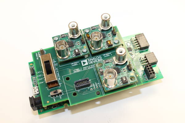
The ADuCM355 on-chip system provides the features needed to bias and to measure a range of different electrochemical sensors. The EVAL-ADuCM355QSPZ allows users to evaluate the performance of the ADuCM355 when implementing a range of different electrochemical techniques, including chronoamperometry, voltammetry, and electrochemical impedance spectroscopy (EIS).
Complete specifications for the ADuCM355 are available in the ADuCM355 data sheet, which must be consulted in conjunction with the EVAL-ADuCM355QSPZ user guide when using the EVAL-ADuCM355QSPZ.
Applicable Parts
ADUCM355
Precision Analog Microcontroller with Chemical Sensor Interface
Applications
Intelligent Buildings
- Environmental Monitoring Solutions
EVAL-ADA4625-1

UG-1201 describes the evaluation board for the ADA4625-1 low noise, fast settling, single supply, rail-to-rail output (RRO), junction field effect transistor (JFET) op amp in an 8-lead small outline integrated circuit (SOIC) package with an exposed pad. The design of this evaluation board emphasizes simplicity and ease of use. This evaluation board is a 2-layer board that accommodates edge mounted SubMiniature version A (SMA) connectors on the inputs and outputs. The SMA connectors allow efficient connection to test equipment or other circuitry.
The evaluation board ground plane, components placement, and power supply bypassing are optimized for maximum circuit flexibility and performance. The exposed pad of the ADA4625-1 is connected to the ground plane on the evaluation board to enhance thermal and noise performance. The evaluation board uses a combination of surface mount technology (SMT) component case sizes 0603 and 0805, with the exception of the bypass capacitors, Capacitor C3 and Capacitor C5, which have a maximum standard size of 1206. The evaluation board also features a variety of unpopulated resistor and capacitor pads, which provide the user with multiple choices and extensive flexibility for different application circuits and configurations, such as active loop filters, transimpedance amplifiers (TIAs), and charge amplifiers.
The ADA4625-1 data sheet covers the specifications and details of the device operation and application circuit configurations and guidance. Consult the data sheet in conjunction with UG-1201 for a better understanding of the device operation, especially when powering up the evaluation board for the first time.
Applicable Parts
ADA4625-1
36 V, 18 MHz, Low Noise, Fast Settling Single Supply, RRO, JFET Op Amp
Applications
EVAL-ADAQ7980

The EVAL-ADAQ7980SDZ is an evaluation board designed to demonstrate the low power ADAQ7980 performance and provide an easy to understand interface for a variety of system applications. The ADAQ7980 is a 16-bit, 1 MSPS, μModule data acquisition system that integrates four common signal processing and conditioning blocks into a system in package (SiP) design that supports a variety of applications
The EVAL-ADAQ7980SDZ can also evaluate the ADAQ7988, despite being populated with the ADAQ7980. To mimic the evaluation of the ADAQ7988 performance, limit the maximum sample rate of the ADAQ7980 to 500 kSPS in the ADAQ798x Evaluation Software.
The evaluation board is ideal for use with the Analog Devices, Inc., system demonstration platform (SDP) board, EVAL-SDP-CB1Z. The EVAL-ADAQ7980SDZ interfaces to the SDP board via a 120-pin connector. P1, P2, P3, and P4 SMA connectors are provided to connect a low noise analog signal source.
The ADAQ798x Evaluation Software executable controls the evaluation board over the USB through the EVAL-SDP-CB1Z. See the Related Links section for a list of on-board components
A full description and complete specifications for the ADAQ7980 are provided in the ADAQ7980/ADAQ7988 data sheet and must be consulted in conjunction with this user guide when using the evaluation board. Full details on the EVAL-SDP-CB1Z are available on the SDP-B product page.
Applicable Parts
Applications
Latest Resources

All Resources
Videos
- ADI's CN0531: Programmable 20-Bit Precision DC Voltage Source
- ADI's LTM8060 40VIN, Quad 3A SILENT SWITCHER® μMODULE REGULATOR
- ADI's ADN4624 5.7 kV rms Quad-Channel 2.5 Gigabit Isolator
- ADIN1100: A Robust, Industrial, Low Power 10Base-T1L Ethernet PHY
- ADAQ23875: 16-Bit, 15 MSPS, μModule® Data Acquisition Solution
Application Notes
- AN-649: Using the Analog Devices Active Filter Design Tool
- AN-713: The Effect of Long-Term Drift on Voltage References
- AN-1329: Noise Reduction Network for Adjustable Low Dropout Regulators (Rev. 0) PDF
- AN-1380: Generating Secondary Fault Supplies for Fault Protected Switches PDF
- AN-892: Temperature Measurement Theory and Practical Techniques (Rev. 0) PDF
Technical Articles
- A 16-bit 16-MS/s SAR ADC With On-Chip Calibration in 55-nm CMOS
-
CTSD Precision ADCs—Part 2: CTSD Architecture Explained for Signal Chain Designers
Analog Dialogue
- From IoT Factories to Operating Rooms: How to Design Better Comms Systems
-
The Interleaved Inverting Charge Pump—Part 2: Implementation and Results
Analog Dialogue
- μModule Data Acquisition Solution Eases Engineering Challenges for a Diverse Set of Precision Applications
Product Selection Guide
Design Tools
Solutions Bulletins & Brochures
Webcasts
Tutorials
- MT-040: Op Amp Input Impedance PDF
- MT-074: Differential Drivers for Precision ADCs PDF
- MT-059: Compensating for the Effects of Input Capacitance on VFB and CFB Op Amps Used in Current-to-Voltage Converters PDF
- MT-093: Thermal Design Basics PDF
- MT-033: Voltage Feedback Op Amp Gain and Bandwidth PDF